Metalens technology is revolutionizing optics in ways we never thought possible. Developed by Rob Devlin and his team at Metalenz, this groundbreaking innovation employs a series of mini-lenses—also known as metasurfaces—to bend and focus light using sophisticated nanostructures. By harnessing the principles of traditional optics while eliminating the bulk of conventional glass lenses, metalens devices are making waves in the consumer electronics market. As Harvard technology transfer efforts facilitate the commercialization of these advanced optical solutions, the potential for optics disruption is becoming a reality. With applications ranging from smartphones to augmented reality, the mini-lens innovation is poised to redefine what we understand about light manipulation and image processing.
The cutting-edge field of metalens technology, also referred to as mini-lens innovation, is at the forefront of a new wave in optics. These advanced optical devices utilize metasurfaces to control light with unprecedented accuracy and miniaturization. By replacing bulky traditional lenses with tiny, efficient solutions, developers are not only enhancing image quality but also enabling new functionalities across various electronic applications. This evolution is backed by significant research from prestigious institutions like Harvard, underscoring the critical role of university knowledge transfer in bringing groundbreaking technologies to market. As the industry shifts toward these advanced optics solutions, the possibilities for electronics, including 3D sensing and facial recognition, are expanding rapidly.
Understanding Metalens Technology and Its Applications
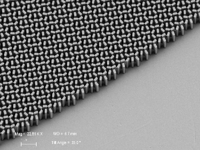
Metalens technology represents a significant advancement in optical engineering, enabling devices to manipulate light at a nanoscale. Unlike traditional lenses, which rely on curved surfaces to focus light, metalenses use a flat surface embedded with nanostructures to bend light. This innovation is not only compact but also cost-effective, making it ideal for integration into consumer electronics. Devices equipped with metalenses can achieve high-performance metrics while reducing the overall footprint of optical systems, thus unlocking new potentials for product designs in smartphones and tablets.
The appeal of metalens technology extends beyond mere size reductions. It opens up possibilities for enhanced functionalities, such as integrating advanced features like depth sensing and augmented reality capabilities in everyday gadgets. Companies like Metalenz are pioneering this technology, with products designed to perform multiple optical tasks simultaneously. This versatility positions metalenses as a key player in the optics disruption movement, pushing the boundaries traditionally set by curved lenses in various applications.
The Role of Harvard Technology Transfer in Metalenz Success
Harvard University’s Office of Technology Development plays a pivotal role in the transformation of groundbreaking research into viable commercial products. The journey of metalens technology from laboratory innovation to mass production exemplifies the effectiveness of this technology transfer model. By providing researchers like Rob Devlin with resources and support, Harvard has helped bridge the gap between academic research and industrial application, allowing ideas with great potential to flourish in the commercial market.
The success of Metalenz can be attributed to collaborative efforts within a multidisciplinary research environment. The foundation laid during Devlin’s time in the Capasso lab not only sparked the innovation of the mini-lens but also demonstrated how university capabilities can spawn numerous products and even new industries. This interaction catalyzes genuine disruption in traditional fields, proving the importance of technology transfer in sparking real-world advancements.
Mini-Lens Innovation: A Fundamental Shift in Optics
The introduction of mini-lens innovations signifies a fundamental shift in the optics industry. By utilizing metasurfaces, these miniature lenses can focus light with greater efficiency than traditional lenses composed of thick glass or plastic. This shift is crucial for manufacturers trying to include more features in handheld devices without increasing their size. Metalenz, leveraging this technology, provides a streamlined solution that meets the demands of modern consumer electronics, which require increasingly complex optical systems in compact forms.
As devices evolve to accommodate higher resolutions and multiple sensors, mini-lenses offer a way to integrate sophisticated optics without compromising design. The use of these innovative components enables manufacturers to enhance functionalities such as camera quality, augmented reality interaction, and facial recognition security. The mini-lens evolution not only redefines the manufacturing processes in the industry but also drives a new wave of consumer expectations for device performance.
The Competitive Edge of Metalenz in the Emerging Market
Metalenz’s early entry into the market has given it a competitive edge over emerging players in the optics sector. With successful partnerships, such as their collaboration with STMicroelectronics, Metalenz has integrated its metasurfaces into essential devices like the FlightSense module. This strong foothold allows them to reap the benefits of first-mover advantage while setting industry standards for metasurface applications in consumer electronics. As competitors strive to catch up, Metalenz focuses on continuous product optimization and innovation, ensuring they stay at the forefront of this rapidly evolving technology.
Rob Devlin acknowledges that maintaining a competitive advantage requires not just initial successes, but an ongoing commitment to research and development. By leveraging the relationships with academic innovators and embracing the latest advancements emerging from the Capasso lab, Metalenz is poised to introduce new functionalities and enhancements in their products. This proactive approach not only secures their position in the optics industry but also encourages further breakthroughs that could create entirely new markets for light manipulation technology.
Exploring Metasurfaces in Electronics: Beyond Optics
Metasurfaces are revolutionizing not only optics but also the broader electronics landscape. These flat surfaces made up of carefully engineered nanostructures enable control over electromagnetic waves, thereby opening up new capabilities in fields like telecommunications and sensor technology. The versatility of metasurfaces extends their utility beyond imaging; they are paving the way for advancements in wireless communication, 3D sensing, and even energy harvesting applications.
The integration of metasurfaces into electronics promises greater efficiency and functionality. With the potential to miniaturize components and reduce costs significantly, manufacturers are exploring how to leverage these technologies to enhance everyday devices. As research proliferates in this area, it is likely that we will see new applications of metasurfaces emerge, further highlighting their value across various sectors of technology.
Impact of Light Manipulation on Augmented Reality Innovations
Light manipulation via metalens technology is transforming the landscape of augmented reality (AR). The ability to control light on small scales allows for more precise interactions in AR environments, enhancing user experiences. For instance, metalenses can facilitate improved image quality and depth perception, essential elements for realistic AR applications. As this technology evolves, the accuracy and immersion of virtual objects within the real world will only improve, laying the groundwork for more sophisticated applications.
Moreover, as device components shrink with innovations like mini-lenses, portable AR devices will benefit from lighter and more energy-efficient options. This accessibility is crucial for broader adoption, opening up new markets for AR applications in fields ranging from gaming to healthcare. As more consumer products incorporate advanced optics such as metalenses, the convergence of AR and everyday life will likely be accelerated, leading to transformative user interactions.
The Future of Optical Systems: Innovations from Metalenz
The future of optical systems lies in the continuous advancement of innovations like those offered by Metalenz. With the company’s current focus on projects like Polar ID, the potential applications for their metasurfaces are expansive. By harnessing the unique properties of light polarization, Metalenz is not only aiming to produce more compact security solutions but also revolutionizing how optical systems function across various industries. This positions them at the forefront of the optical technology landscape, ready to address tomorrow’s challenges.
As Metalenz continues to evolve, the implications of their innovations extend to various fields beyond consumer electronics. Applications in healthcare, environmental monitoring, and security are on the horizon, showcasing how light manipulation can enhance existing technologies. By pushing the boundaries of what optics can achieve, companies like Metalenz are essential in shaping a future where advanced optical systems are commonplace in our daily lives.
Rob Devlin and the Vision Behind Metalenz
Rob Devlin’s leadership has been instrumental in shaping the vision behind Metalenz. With his background in materials and nanofabrication, Devlin has successfully guided the company in translating its cutting-edge research into practical, commercially viable products. His commitment to harnessing transformative technologies reflects a broader ethos within the startup community, where academic insights catalyze the formation of new industries.
Devlin’s perspective that innovative technologies should be accessible in everyday devices underscores the importance of democratizing advanced optics. His emphasis on collaboration with researchers at Harvard ensures that the startup remains connected to groundbreaking developments, enabling Metalenz to maintain its competitive edge and leadership in the optical innovation space. As Devlin and his team navigate the complexities of the evolving tech landscape, their forward-thinking approach will likely yield impactful advancements for years to come.
Challenges and Opportunities in the Metasurface Market
As with any groundbreaking technology, the emergence of metasurfaces poses both challenges and opportunities. Competing entities are increasingly recognizing the potential of metalens technology, prompting an influx of research and development efforts across the optics landscape. While this competition drives innovation and improvements in product offerings, it also necessitates that pioneers like Metalenz continuously adapt and enhance their solutions to remain at the forefront.
The rapidly evolving nature of the market presents unique opportunities for those engaging with metasurface technologies. Companies specializing in these innovations can explore diverse applications beyond traditional optics, venturing into new realms like telecommunications and smart sensor integrations. By leveraging their foundational research into practical solutions, businesses have the chance to redefine industry standards and craft a legacy of innovation that resonates across different technology sectors.
Frequently Asked Questions
What is metalens technology and how does it differ from traditional optics?
Metalens technology refers to innovative devices that use metasurfaces to focus light, differing from traditional optics which rely on bulky glass or plastic lenses. These mini-lenses, developed through advanced nanostructures, are significantly smaller, cheaper, and easily mass-produced, making them ideal for modern consumer electronics.
How has Metalenz’s mini-lens innovation impacted consumer electronics?
Metalenz’s mini-lens innovation has revolutionized consumer electronics by integrating lightweight and compact metasurfaces into devices like smartphones and tablets. Their technology allows for advanced features such as 3D sensing and improved camera functionalities without the need for large lenses, thus enabling sleeker and more powerful gadgets.
What role do metasurfaces in electronics play in modern technology?
Metasurfaces in electronics serve as crucial components for manipulating light at unprecedented scales. They enhance functionalities in various applications, including facial recognition, augmented reality, and depth mapping, all of which rely on precise light control enabled by metalens technology.
How did Rob Devlin contribute to the development of metalens technology at Harvard?
Rob Devlin, during his doctoral studies at Harvard, contributed significantly to the creation of metalens technology by developing and refining the mini-lens design using advanced materials and nanofabrication techniques. His work in Professor Capasso’s lab helped transition the technology from research prototypes to real-world products through the establishment of Metalenz.
What is the significance of Harvard’s technology transfer in the context of Metalenz?
Harvard’s technology transfer has been pivotal for Metalenz, providing a framework for translating cutting-edge research into practical applications. This process enabled the commercialization of metalens technology, allowing innovations from the Capasso lab to significantly disrupt traditional optics markets and create new industries.
What potential advancements can we expect from metalens technology in the future?
Future advancements in metalens technology may include enhanced functionalities like the Polar ID system, which leverages light polarization for improved security in smartphones. Furthermore, ongoing research may lead to applications in environmental monitoring and medical diagnostics, showcasing the versatility and potential of metasurfaces.
Are there competitors in the metalens technology market, and how is Metalenz positioning itself?
Yes, there are competitors in the metalens technology market. However, Metalenz is positioning itself by continuously enhancing its existing products and proactively developing innovative applications for metasurfaces. Their collaborative partnership with researchers at Harvard also provides a significant advantage in maintaining a lead in this rapidly evolving industry.
How does Metalenz manufacture its devices, and what advantages does this provide?
Metalenz outsources the manufacturing of its devices to large semiconductor foundries, which allows for high-volume production of their metalens technology at scale. This approach reduces costs and facilitates faster market entry, as foundries already produce trillions of chips annually, ensuring efficiency and reliability in production.
| Key Point | Details |
|---|---|
| Origin of Metalenz | Developed from research at Harvard under Professor Federico Capasso. |
| Mini-lens Production | Produces millions of metasurfaces for consumer electronics, with demand increasing. |
| Integration in Devices | Used in devices such as iPad, Samsung Galaxy S23 Ultra, and Google Pixel 8 Pro. |
| Key Achievements | Signed a contract with STMicroelectronics to integrate metasurfaces into 3D sensing modules. |
| Polar ID Technology | Next big advancement using polarization for enhanced security at reduced costs. |
| Future Prospects | Focus on enhancing existing products and exploring new functionalities. |
Summary
Metalens technology is transforming the landscape of optics by introducing a new generation of ultra-thin lenses that are fundamentally changing how we think about image capturing and light manipulation. Developed through innovative collaboration at Harvard, metalens technology allows for significant miniaturization of optical devices, making them cheaper and more efficient. Companies are rapidly adopting these technologies for use in high-demand consumer electronics, and emerging advancements like the Polar ID are set to further revolutionize the industry by enhancing security features at a fraction of the traditional cost. As competition intensifies, Metalenz is well-poised to lead the charge into a new era of optical technology.